There comes a moment in every electronics hobbyist’s life when the breadboard starts looking less like a prototype and more like a crime scene. Jumper wires snake everywhere. One loose connection ruins your afternoon. A resistor is hiding under a microcontroller like it owes money. That is usually the moment you start thinking, “Maybe I should make a printed circuit board.” Good instinct. Even better: you do not always need to wait a week, pay shipping, or explain to your future self why you ordered five boards with the LED footprint backward.
The toner transfer PCB method is one of the classic ways to make a custom printed circuit board at home. It uses a laser printer, transfer paper, heat, copper-clad board, and chemical etching to create copper traces for your circuit. Is it as polished as a professionally fabricated PCB with solder mask, silkscreen, plated through-holes, and factory-perfect edges? No. Is it fast, cheap, surprisingly accurate, and deeply satisfying? Absolutely. It is the garage-band version of PCB fabrication: a little messy, occasionally loud, but capable of producing something genuinely useful.
This guide explains how to take your PCBs from good to great using toner transfer. We will cover the process, materials, design rules, common mistakes, safety, finishing techniques, and hard-won practical experience. By the end, you will know how to make sharper traces, avoid undercutting, improve toner adhesion, and produce boards that look less like a science fair emergency and more like something you would proudly solder on.
What Is Toner Transfer PCB Making?
Toner transfer is a DIY PCB fabrication process where you print your circuit layout with a laser printer, transfer that toner onto a copper-clad board, and use the toner as a resist during chemical etching. The exposed copper dissolves in the etchant, while the copper protected by toner remains as your circuit traces.
The key detail is that laser printer toner is not ink. It is a plastic-like powder fused onto paper by heat. When reheated against clean copper, it can soften and stick to the board. That stuck toner becomes a temporary shield. The etchant attacks the bare copper, but the toner-covered copper survives. After etching, you remove the toner, drill holes if needed, clean the board, and solder components.
Why hobbyists still love it
Professional PCB services are affordable and excellent, but toner transfer still earns its place on the bench. It is ideal when you need one board today, not “after tracking information becomes emotionally available.” It is also great for quick analog circuits, adapter boards, test fixtures, LED projects, simple microcontroller boards, and educational experiments.
The biggest benefit is speed. Once your layout is ready, a single-sided board can often go from printout to soldering in the same evening. That rapid feedback loop helps you learn PCB design faster. Nothing teaches trace spacing, pad size, drill accuracy, and component placement quite like physically building the thing you just designed.
The Basic Toner Transfer Workflow
The process is simple in theory, but the quality comes from details. Think of toner transfer like making pancakes: the ingredients are basic, but the first one may look like it lost a wrestling match.
1. Design the PCB layout
Start with PCB design software such as KiCad, Eagle, EasyEDA, or another layout tool. For home toner transfer, keep the design realistic. Use wider traces when possible, generous pads, and practical spacing. If you are just beginning, avoid tiny fine-pitch components unless you enjoy debugging with a magnifier and muttering.
For reliable home results, use traces around 10 mil or wider when the design allows. Larger power traces are even better. Keep enough spacing between traces to prevent copper bridges after etching. Make pads slightly larger than you would for a factory board, especially for through-hole parts. Your drill bit does not care about your confidence; it cares about physics.
2. Print the artwork correctly
Use a laser printer, not an inkjet printer. Inkjet ink will not form a durable etch resist in this process. Print at the highest density or darkest setting available. Turn off toner-saving mode. If your software has scaling settings, print at 100 percent size. A tiny scaling error can turn an integrated circuit footprint into modern art.
For single-sided boards, print the copper layer mirrored if required so the transferred image lands in the correct orientation. For double-sided boards, alignment becomes more demanding, so add registration marks and test the process on paper before committing to copper.
3. Choose the right transfer paper
Transfer paper matters more than beginners expect. The goal is to hold toner just well enough to print cleanly, but not so well that it refuses to release onto copper. Glossy magazine paper, dedicated toner transfer paper, certain photo papers, and backing sheets from labels are common options. Dedicated transfer paper is often more predictable, but many makers successfully use inexpensive glossy paper.
The perfect paper is the one that works with your printer, laminator or iron, board material, and patience level. Test small patterns before printing your masterpiece. Include thin traces, ground fills, text, and pads in your test strip. It will reveal problems faster than sacrificing a full board.
4. Prepare the copper like your project depends on it
Because it does. Copper preparation is where good boards become great boards. Toner sticks best to clean, oxide-free, oil-free copper. Fingerprints, dust, oxidation, paper fibers, and mysterious bench grime can all create pinholes or missing traces.
Scrub the copper-clad board gently with a fine abrasive pad until the surface is evenly bright. Wash it with dish soap and water, rinse thoroughly, and dry it without touching the copper. Some makers wipe the surface with isopropyl alcohol after cleaning. Handle the board by the edges or wear gloves. Your fingertips are excellent at leaving invisible sabotage.
Heat Transfer: Iron vs. Laminator
The transfer step uses heat and pressure to move toner from paper to copper. You can do this with a household clothes iron or a modified laminator. Both can work. Both can also humble you.
Using a clothes iron
A clothes iron is cheap and available, but it can be inconsistent. The temperature varies across the soleplate, pressure depends on your hand, and steam holes can create uneven contact. If you use an iron, turn off steam, use a firm surface, and apply steady pressure across the whole design. Move slowly and avoid sliding the paper around.
Small boards are easier with an iron than large boards. For larger PCBs, the edges may transfer well while the center remains patchy, or the center may cook while the edges sulk. Preheating the copper board slightly can help. So can placing plain paper above the transfer paper to distribute pressure.
Using a laminator
A laminator offers more consistent pressure and repeatable heat. Many hobbyists prefer it because the board passes through rollers evenly. Some laminators need modification to run hot enough or accept thicker copper-clad board. Others work well out of the box with repeated passes.
The laminator method shines when you want repeatability. Once you find the right paper, temperature, and number of passes, you can reproduce results more easily. That does not mean every board will be perfect. It means your failures become more scientifically annoying instead of completely random.
Soaking and Removing the Paper
After heating, let the board cool slightly, then soak it in warm water. The water softens the paper so it can be peeled or rubbed away. Go slowly. If you tear the paper off aggressively, you may also pull toner off the copper. The goal is to remove paper fibers while leaving the toner pattern intact.
Some papers release cleanly in sheets. Others dissolve into a fuzzy pulp that requires gentle rubbing with your thumb. Be patient. If a thin film remains over the toner, that may be fine. If paper fibers remain between traces, remove them carefully because they can interfere with etching.
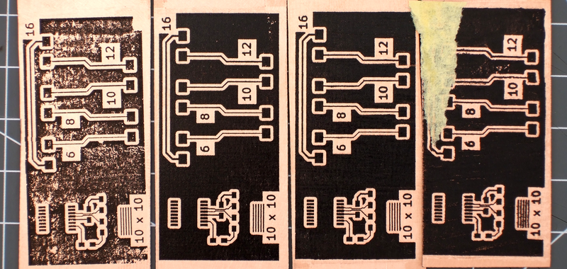
Inspect the board under strong light. Look for broken traces, pinholes, smeared pads, and accidental bridges. Tiny gaps can be repaired with an ultra-fine permanent marker or etch-resist pen. Large missing sections are usually a sign to clean the board and try again. There is no shame in restarting. There is shame only in pretending a broken ground trace is “probably fine.” It is not fine. It is waiting.
Etching the PCB
Etching removes the copper that is not protected by toner. Common PCB etchants include ferric chloride and ammonium persulfate. Ferric chloride is popular because it is widely available, effective, and reusable, but it stains aggressively and should be treated with respect. Use gloves, eye protection, ventilation, and a non-metallic container. Do not use your favorite kitchen bowl unless you enjoy explaining chemistry to your family.
How to get cleaner etching
Agitation helps fresh etchant reach the copper surface. Gently rock the container or use a safe etching tank setup. Warmer etchant usually works faster than cold etchant, but do not overheat chemicals or improvise unsafe heating methods. Follow the etchant manufacturer’s directions. Faster is not always better; aggressive etching can undercut traces and reduce detail.
Undercutting happens when the etchant eats sideways under the toner resist. This can make traces thinner than designed, especially during long etch times. To reduce undercutting, use fresh or properly maintained etchant, avoid extremely thin traces, keep copper areas balanced, and remove the board as soon as the unwanted copper is gone.
Watch the board, not the clock
Etch time depends on copper thickness, etchant strength, temperature, agitation, and how much copper must be removed. A board with large copper pours removed may take longer than a board with mostly isolated traces. Check progress frequently. When the exposed copper is gone, remove the board and rinse it thoroughly in water according to safe handling practices.
Removing Toner, Drilling, and Finishing
Once etching is complete, remove the toner resist. Acetone often works well, but use it safely, away from flames, with ventilation. After the toner is removed, the copper traces should be visible and shiny. Inspect again for bridges or breaks. A continuity tester is your friend here. It does not judge. It only beeps.
Drilling holes
For through-hole boards, drilling is the next major step. A small drill press or rotary tool stand gives much better results than freehand drilling. Use sharp carbide bits if available, and wear eye protection. Drill pads should be large enough to survive slight misalignment. If your pads are tiny, the drill bit may remove them entirely, leaving you with a philosophical question instead of a solder joint.
Tinning and protecting copper
Bare copper oxidizes over time. For better solderability, you can tin the traces with solder or use a chemical tinning solution designed for PCBs. Flux helps solder flow cleanly. After soldering, clean flux residue if needed and consider applying a protective coating. DIY boards usually lack solder mask, so stray solder bridges are easier to create. Slow down and use the right amount of solder.
Design Rules That Make Toner Transfer Easier
Great toner transfer begins before the printer warms up. The board layout should respect the limits of your home process. You can push limits later, but start with designs that want to succeed.
Use friendly trace widths
For beginner boards, wider traces are better. Signal traces around 10 to 16 mil are usually more forgiving than very fine traces. Power traces should be wider based on current needs. If the circuit has room, use it. Empty board space does not earn bonus points.
Increase pad sizes
Larger pads make drilling and soldering easier. This is especially important for connectors, switches, headers, and components that experience mechanical stress. A pad that looks elegant on screen can become a copper donut tragedy after drilling.
Avoid unnecessary complexity
Single-sided boards are easiest. Double-sided toner transfer is possible, but alignment is harder and vias are not plated. You may need wire jumpers or manually soldered via wires. This is not a failure; it is a practical design choice. A neat jumper wire beats a misaligned double-sided board every time.
Use ground pours wisely
Ground pours reduce the amount of copper that must be etched, which can shorten etch time and reduce etchant exhaustion. They can also improve electrical performance in some designs. However, keep adequate clearance around traces and pads. Poorly planned pours can create tiny gaps that trap paper fibers or form copper whiskers.
Common Toner Transfer Problems and Fixes
The toner does not stick
Likely causes include dirty copper, insufficient heat, insufficient pressure, incompatible paper, or low toner density. Clean the board more thoroughly, increase transfer time carefully, adjust printer settings, or test a different paper.
Traces are smeared
The paper may have shifted during transfer, or the toner overheated and spread. Tape the paper securely, avoid sliding pressure, and reduce heat or transfer time slightly.
Fine traces have breaks
This can come from poor toner density, paper fibers, oxidation, or rough handling during paper removal. Print darker, clean better, soak longer, and inspect before etching. Touch up small defects with an etch-resist marker.
Copper bridges remain after etching
The spacing may be too tight, etching may be incomplete, or toner may have smeared between traces. Continue etching only if copper is clearly still present, but avoid over-etching. After etching, tiny bridges can sometimes be cut with a sharp blade.
Pads lift during soldering
DIY etched boards do not have plated through-holes or the same adhesion advantages as manufactured boards. Use moderate heat, avoid repeated rework, and make pads larger in the next revision.
Safety: The Part That Keeps the Hobby Fun
Toner transfer involves heat, sharp tools, solvents, and chemical etchants. Treat the process like real fabrication, not arts and crafts with extra electrons. Wear safety glasses when cutting, drilling, and handling chemicals. Use gloves with etchants and solvents. Work in a ventilated area. Label containers clearly. Keep chemicals away from children, pets, food, and anyone who thinks “What happens if I touch this?” is a personality.
Never pour used etchant down the drain. Spent PCB etchant contains dissolved copper, and disposal rules vary by location. Store used etchant in a compatible, labeled container and take it to an appropriate hazardous waste facility or follow your local waste authority’s instructions. The board may be small, but the environmental responsibility is not.
When Toner Transfer Is the Right Choice
Toner transfer is excellent for fast prototypes, one-off circuits, educational builds, repair adapters, and simple through-hole or modest surface-mount projects. It is also useful when you want to understand how PCBs physically work. Designing a board is one skill; fabricating it teaches another layer of reality.
However, toner transfer is not always the best choice. If you need plated through-holes, solder mask, controlled impedance, fine-pitch BGAs, multi-layer routing, tight manufacturing tolerance, or dozens of identical boards, send the design to a PCB manufacturer. The goal is not to prove you can do everything at home. The goal is to choose the process that fits the job.
From Good to Great: Practical Toner Transfer Upgrades
If your boards already work but look rough, small improvements can make a big difference. Start by standardizing your process. Use the same printer, paper, board type, cleaning method, transfer method, etchant, and timing notes. When something improves, you will know why.
Create a test coupon
Before making an important board, print and transfer a small test coupon with different trace widths, spacing, text sizes, and pad styles. This tells you what your process can actually reproduce. Your printer may claim impressive resolution, but copper has opinions.
Preheat and dry the board
Moisture can interfere with transfer quality. Some makers warm the copper board before transfer to remove moisture and improve toner adhesion. Do this carefully and consistently. The aim is warm and dry, not “why does the bench smell weird?”
Use registration marks for double-sided boards
For double-sided toner transfer, add alignment holes or marks outside the circuit area. Tape the two printed layers into a pocket, slide the board inside, and check alignment against a bright light. Expect some trial and error. Double-sided home PCBs are possible, but they reward patience more than optimism.
Design for inspection
Add labels, test pads, and clear polarity markings when possible. Even if you do not have silkscreen, you can place etched text in copper or keep a printed assembly diagram nearby. Future you will appreciate not having to guess which header pin is ground while holding a hot soldering iron.
Experience Notes: What Actually Makes Toner Transfer Better
After making a few toner transfer PCBs, one lesson becomes painfully clear: the transfer step gets all the attention, but the boring steps decide the outcome. Cleaning the copper is not glamorous. Nobody writes heroic songs about scrubbing oxidation. Yet most failed transfers begin with a surface that was almost clean, which is another way of saying not clean enough. The copper should look evenly fresh, not patchy, cloudy, or fingerprinted. If you clean it perfectly and then touch it with bare fingers, congratulations, you have invented a small, greasy problem.
The second lesson is that “more heat” is not a universal solution. Beginners often respond to weak toner adhesion by pressing harder and heating longer. Sometimes that works. Sometimes it creates fat traces, smeared pads, and toner that looks like it tried to escape. Better results usually come from balancing heat, pressure, time, and paper type. A laminator can make this easier because it removes some human randomness. With an iron, consistency is harder, so mark your settings, use the same surface, and practice on small boards.
Paper choice is another rabbit hole. One glossy paper releases beautifully; another clings like it has abandonment issues. Some magazine papers work well, but the coating varies. Dedicated toner transfer paper costs more but can save time. The best approach is to test several papers with the same small layout. Include thin traces, large filled areas, and small text. If small text transfers cleanly, your process is probably healthy.
Etching teaches patience. Pull the board too early and copper islands remain. Leave it too long and traces shrink from undercutting. The sweet spot is active observation. Gently agitate, check progress, and remove the board once the exposed copper is gone. Large copper pours help because they reduce the amount of copper that must dissolve. They also make the board look more professional, which is always nice when you are showing someone a rectangle you attacked with chemicals.
Drilling is where many good boards lose points. A beautiful etched board can become ugly if the holes wander. Use a stand if possible, choose the right bit size, and make pads generous. For connectors and parts that will be plugged, unplugged, or mechanically stressed, bigger pads and thicker traces are not ugly; they are survival features. If a trace breaks, do not panic. Small repairs with wire jumpers are normal in prototypes. Even commercial engineering labs have bodge wires. They simply use nicer microscopes while pretending it was part of the plan.
The final experience-based advice is to keep notes. Record the printer, paper, heat method, number of laminator passes, board cleaning method, etchant condition, and results. Toner transfer has many variables, and memory is a terrible lab notebook. Once you find a combination that works, protect it like a secret family recipe. Great toner transfer is not magic. It is repeatability wearing safety glasses.
Conclusion
The toner transfer PCB method remains one of the most useful skills for electronics hobbyists, makers, students, and rapid prototypers. It is inexpensive, fast, educational, and flexible enough for many practical circuits. More importantly, it turns PCB fabrication from a mysterious factory process into something you can understand with your own hands.
To take your PCBs from good to great, focus on the fundamentals: clean copper, dark laser printing, reliable transfer paper, consistent heat and pressure, careful etching, safe chemical handling, and design rules that match your process. Wider traces, larger pads, good spacing, ground pours, and patient inspection will improve results dramatically.
Toner transfer is not a replacement for professional PCB manufacturing, and it does not need to be. It is a fast, hands-on method for learning, experimenting, and building boards when waiting feels like the least fun option. With practice, your DIY PCBs can become cleaner, sharper, and more dependable. They may not have glossy solder mask or factory silkscreen, but they will have something better: the quiet satisfaction of knowing you made the board yourself, and it actually works.